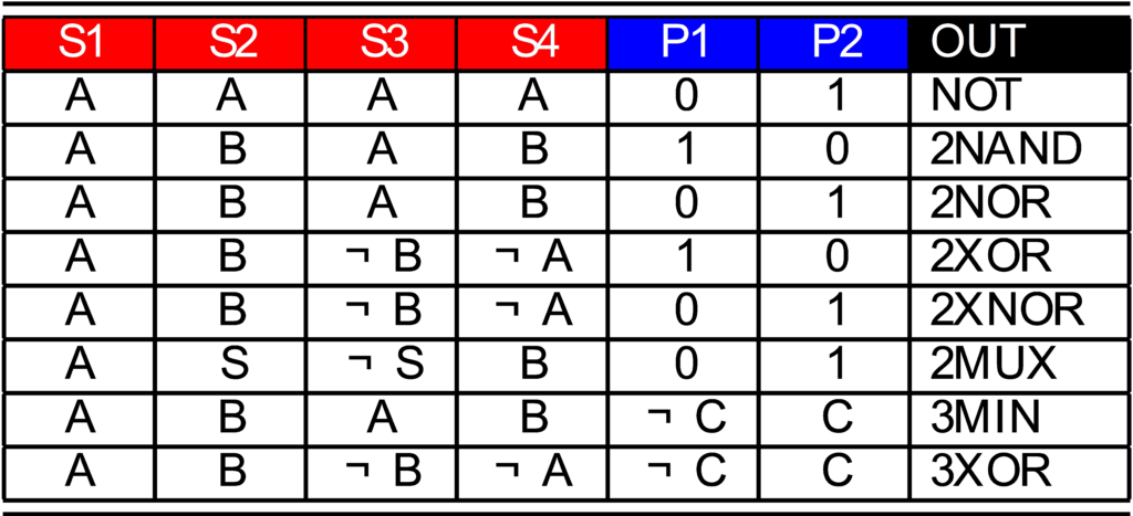
The multiple operation states of reconfigurable FETs open up new opportunities for logic circuit design. Mainly, two features that were previously not accessible with conventional FETs are currently being studied. First, runtime-reconfigurable logic gates can be built, providing multiple functionalities as programmed on-the-fly by volatile select signals. One basic example is given by the compact cell, that can switch from NAND to NOR operation. Distinctly, those cells always operate in a complementary manner, reaching a full swing output and exhibiting the same delay for both functions. The second feature is the integration of multiple gate electrodes along the channel, merging paths of series transistors within a single one, without increasing the internal resistance of the individual device. This feature can be exploited to build efficient XOR and Majority gates. Both features can be combined to yield a logic gate built from four transistors able to map 8 different functionalities (Fig. 1).
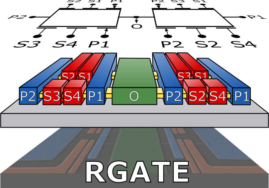
This so-called RGATE (Fig. 2) shows prominence for hardware security applications, predominantly due to two features: functionality polymorphism and structural polymorphism. Just by looking at the cell layout, it is impossible to retrieve their underlying electrical functionality. This polymorphic nature enables new approaches on hardware security solutions, such as logic locking, camouflaging, physically unclonable functions (PUFs), or chip authentication. Considering careful gate level design solutions, it is even possible to equalize the propagation delay of two related operational modes of a NAND/NOR reconfigurable logic gates, leading to near delay-invariant designs. The remaining differences in the delay traces is well hidden by the influence of process fluctuations, suggesting a high application potential in the field of securing circuits against timing side-channel-attacks.
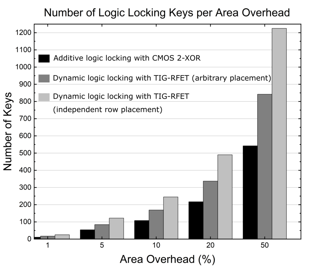
One particular hardware security option with RFETs is to utilize the dynamic reconfigurable gates for logic locking. Here, instead of inserting additional XOR gates to a circuit design, existing gates are replaced by the polymorphic gates. This way the area overhead can be smaller. Also, it is not possible to strip the logic lock from the original design. First analysis on the ISCAS-85 benchmark have revealed that up to twice the number of keys can be added with this technique to any given design while keeping the same area overhead (Fig. 3).

Cooperation:
cfaed – Center of Advancing Electronics Dresden (Germany), TU Darmstadt (Germany), KIT (Germany), Universität Bremen (Germany), GlobalFoundries (Germany), TH Mittelhessen (Germany)