Research Areas
Many major advances in micro- and nanoelectronics have been driven by the introduction of new materials into the fabrication process, such as strained SiGe channels, high-k dielectrics, and copper metal connections in the back-end-of-line. Originally, NaMLlab was created to explore new high-k materials for future generations of nanoelectronic devices, especially for memory applications. This topic is still at the heart of NaMLab. Due to the incredible success of novel ferroelectric devices in opening new directions in device development, ferroelectrics have become the most important topic in material development at NaMLab. Further, this know-how in materials for microelectronic devices has become the foundation for the other six research areas currently pursued at Namlab.
Contact

Prof. Dr.-Ing. Thomas Mikolajick
Scientific Director





Materials for Microelectronic Devices
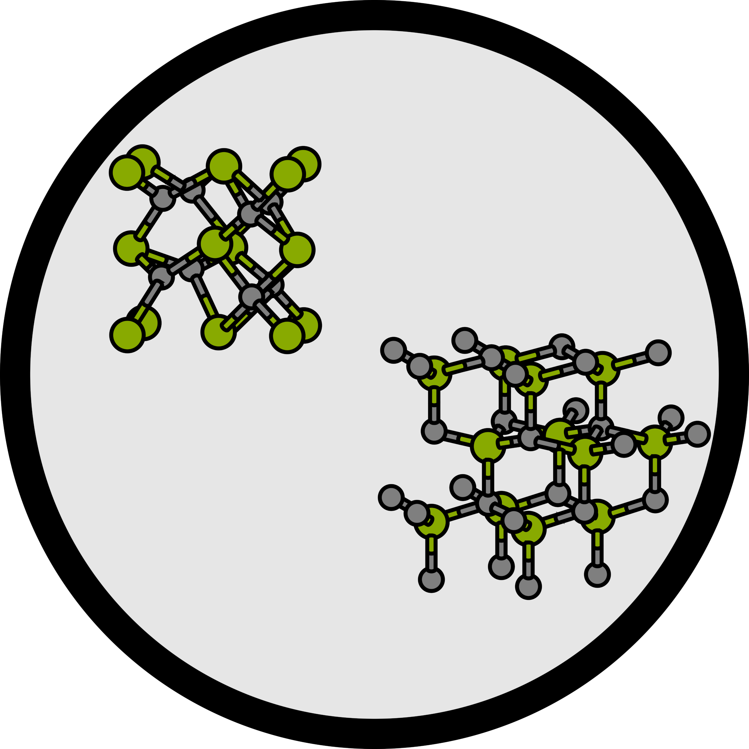
The list of evaluated dielectric and ferroelectric materials includes fluorite-structured ferroelectric materials, such as doped HfO2 with dopants ranging from elements smaller than Hf or Zr, such as Si and Al, to dopants larger than Hf/Zr, including Sc, Y, La, and Sr. Here, dopants can be 3- to 5-valent. For implementation in ferroelectric devices, the thickness of the doped HfO2 layers must be reduced to 5 nm or less. For capacitor fabrication, a long list of electrode materials is screened, including pure metals like W, Pt, Ti, metal nitrides like TiN, TaN, NbN, and metal oxides like RuOx, IrOx, WOx.New materials are also relevant in the area of power electronics. Here the material focus is on GaN. NaMLab intensively explores the growth of GaN and related compounds by HVPE and MBE, and also uses MOVPE for special applications. Moreover, novel dielectrics are integrated with wide-bandgap materials, such as GaN and SiC. Related to both previously described fields is the field of wurtzite-structured.

Non-Volatile Memories
The scaling of conventional silicon-based memories, such as Dynamic random-access memory (DRAM) and Static random-access memory (SRAM), has approached and even surpassed the 10 nm technology node, and NAND Flash memory (NAND) transitioned to 3D stacked memory cells. Further miniaturization faces serious physical limits. A constantly increasing performance gap between stand-alone DRAM and NAND Flash offers a great opportunity for emerging non-volatile memory devices to advance, thus helping sustain the pace of continuous performance improvement at the system level. Moreover, the increased complexity of modern CMOS processes makes the integration of traditional transistor-based embedded non-volatile memories more challenging and less cost-effective. Thus, memory cells with the important storage element in the back-end-of-line are highly desirable for embedded memories.
New Computing Hardware
Ever since the invention of the Integrated Circuit in 1976, classical digital computing has been built on MOSFET transistors, which switch reliably between two states to represent information strictly with 1s and 0s. New computing paradigms move beyond fixed, sequential, and CPU-centric processing toward models that are parallel, adaptive, distributed, and often inspired by nature or intelligence itself. Unlike classical computing, which excels at deterministic and well-defined problems, these new approaches (including AI-native, quantum, edge, and neuromorphic computing) are designed to handle massive amounts of data, uncertainty, and real-time decision-making. Another major benefit of new computing paradigms is that the same amount of data can be processed with fewer elements, leading to smaller and more energy-efficient electronic systems. Such systems are needed because modern societal challenges, including climate modeling, healthcare, smart infrastructure, and global-scale communication, exceed the performance, energy efficiency, and scalability limits of traditional systems. At Namlab, we research emerging electronic elements that enable new computing paradigms as well as their integration into larger systems.


Power Electronics
Climate change is the most critical global challenge our society is facing. Achieving net-zero CO2 emissions by 2050 requires innovations in at least three major areas: mobility, renewables, and information technology. All these areas rely on power electronics, which are essential for converting, controlling, and conditioning electrical energy. For instance, high-efficiency and high-density power converters are critical for charging electric vehicles, avoiding the waste of energy harvested from renewables, and supporting the data center revolution driven by artificial intelligence. Silicon (Si)-based devices, such as the insulated-gate bipolar transistor and the superjunction metal-oxide-semiconductor field-effect transistor, dominate power electronics. The performance of power electronic devices greatly depends on the intrinsic material properties of the semiconductor used to realize the devices. Compared to Si, wide-bandgap semiconductors offer several advantages, including higher thermal conductivity, greater breakdown field, as well as lower conduction and switching losses; thus, opening disruptive perspectives for power electronics. Gallium nitride (GaN) has emerged as one of the most promising wide-bandgap semiconductors for power electronics, opening the way for devices that can significantly outperform their Si-based counterparts in high-frequency power switching applications. GaN power electronic devices can operate at higher frequencies, temperatures, and blocking voltages than those based on Si, while providing substantially higher system efficiencies in a smaller area footprint. NaMLab focuses on bridging fundamental and applied research on GaN crystal growth, process development and device technology to advance the realization of next-generation high-efficiency and high-density power converters.
Modelling and Design-Technology-Co-Optimization
The research on new materials and device concepts comes along with the development of suitable and often unconventional electrical operation schemes. For example, in order to alter the state of a memory device, suitable voltage or current pulses have to be applied. Both, amplitude and timing as well as the order of versatile switching pulses applied to the memory devices have an impact on their electrical performance and reliability on system level. Moreover, due to the very different device configurations with two, three or even more terminals, the memory array architectures and corresponding readout schemes differ even more significantly. For example, dc-currents ranging from pico-Ampere up to some 10 of mircro-Ampere (10-12 – 10-5 A) have to be sensed when reading FeFETs, FTJs or ReRAM devices while polarization switching charges down to some femto-coulomb (10-14 C) have to be sensed when reading FeCAPs. Moreover, novel reconfigurable transistors (RFET) that can be switched between n- or p-FET mode or even memory modes require the development of entirely new circuits on logic gate level as a prerequisite for their utilization on system level. In our research we follow the concepts of Design-Technology-Co-Optimization (DTCO) and System-Technology-Co-Optimization (STCO), which covers all aspects from novel device characterization and modeling over the design of suitable circuits, CMOS integration of our emerging devices and finally the electrical characterization up to the system level.


Electrical Characterization
Electrical measurements are essential for the characterization of the materials, electronic devices and circuits. Thus, besides the manufacturing of novel materials and devices in our own in-house cleanroom, electrical characterization is one of our main expertise. NaMLab owns four well-equipped electrical characterization labs and offers a large spectrum of electrical characterization techniques.We develop and utilize a broad spectrum of electrical measurement techniques and analysis methods. This includes capacitance measurements, such as C(V), C(T) and C(f) or dc-current measurements with down to femto-Ampere resolution at temperatures between 5 K and 450 K and voltages up to 3000 V. RF-characterization techniques up to 40GHz range are utilized for transistor characterization. Moreover, versatile dynamic pulsed measurement schemes are adopted to characterize memory and logic devices and to develop suitable operation schemes for their application in logic circuits, memory arrays or even combined compute-in-memory concepts. Thereby, mixed digital- and analogue characterization techniques are realized using source- and pulse-measurement-units (SMU, PMU) together with digital control units and dedicated micro-controllers. Sample sizes from some mm² up to 300mm wafers can be handled in different semi- and fully automatic wafer probe-stations by direct probing using single probes, probe cards or special RF-probes. Finally, package level testing can be performed under special temperature and atmospheric conditions for long-term reliability characterization.
Clean Room
NaMLab operates a 330 m² cleanroom facility, featuring ISO Class 6 general working areas and ISO Class 5 lithography areas. The facility supports the fabrication and processing of emerging materials and semiconductor devices, from simple thin-film depositions to complex back-end-of-line (BEOL) processing of functional devices on CMOS substrates. A broad range of fabrication techniques are available, including physical and chemical vapor deposition (PVD/CVD), atomic layer deposition (ALD), electron-beam and laser lithography, reactive ion etching (RIE), and rapid thermal annealing (RTA). Complementary structural characterization techniques, such as ellipsometry and X-ray diffraction (XRD), enable detailed material and device analysis. The flexible cleanroom infrastructure supports process development, device prototyping, and heterogeneous integration, bridging fundamental materials research and functional device demonstrations.