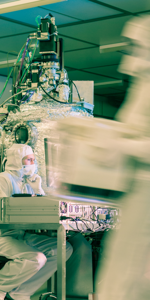
NaMLab is organized as a non-profit limited liability company (gGmbH), but at its core it is a research and technology organization (RTO), located in Dresden, at the heart of the European semiconductor ecosystem. As a TU Dresden company, NaMLab connects academic research with industrial application. Our work focuses on novel electronic devices and covers the entire chain from materials and process development to device fabrication, electrical characterization, and modeling, up to their operation in circuits and systems. Partners from academia and industry benefit from our own cleanroom, our characterization labs, and our experienced teams of senior scientists. Whether you are planning a joint research project, need a tailored investigation of a specific research question, or require a dedicated measurement or processing service, NaMLab offers flexible forms of collaboration: collaborative research projects, direct contract research, and industry services.
Collaborative Research Projects
NaMLab is an experienced partner in publicly funded projects, ranging from fundamental research to application-oriented joint projects with industrial partners. We can participate in a variety of funding schemes offered by the German Research Foundation (DFG), the Federal Ministry of Research, Technology and Space (BMFTR), the Sächsische Aufbaubank (SAB), and the European Union (EU). In fields that match our core research areas, NaMLab also coordinates projects and consortia. Current examples are the European projects SENSOTERIC, which develops a smart sensor analog front-end based on emerging reconfigurable devices, and FIXIT, which develops an ultra-low-power ferroelectric computing platform. Beyond that, NaMLab participates in the DFG Collaborative Research Center/Transregio TRR 404 “Active-3D”, led by NaMLab’s parent university TU Dresden together with RWTH Aachen. Whether as a partner or coordinator, NaMLab contributes its expertise across the entire chain from materials to devices and circuits, from fabrication in our own cleanroom to electrical characterization and modeling. If you are preparing a proposal and are looking for a partner in material-oriented device research, feel free to contact us.


Direct Contract Research
In addition to publicly funded projects, NaMLab offers direct contract research for companies and other third parties. Building on our expertise along the entire chain from materials to devices, we address questions ranging from the evaluation of new materials and process development to the fabrication and characterization of test structures and device demonstrators. Each project is defined jointly with the client, and its scope, deliverables, and confidentiality are agreed individually. Our cleanroom supports process development in both front-end-of-line and back-end-of-line stages and allows hybrid fabrication schemes with partners on wafers up to 200 mm. Contact us to discuss how we can support you with a tailored research and development solution.
Industry Services
NaMLab offers a wide range of technologies and processing services for industry, tailored to specific requirements. From simple thin-film depositions to complex back-end-of-line (BEOL) processing of functional devices on CMOS substrates, our capabilities support both basic material preparation and advanced device processing.
Our 330 m² ISO class 6 cleanroom is equipped for thin-film deposition using PVD, ALD, CVD, and MBE, as well as thermal treatments up to 1200 °C. Micro- and nanostructures can be fabricated using shadow masks, electron-beam and laser lithography, and wet or reactive-ion etching (RIE). We offer the deposition of doped HfO₂ and ZrO₂ films by ALD or PVD on substrates up to 200 mm in diameter, with a wide choice of dopants and electrode materials, as well as subsequent annealing and patterning. In electrical characterization, our four dedicated labs offer capacitance and DC current measurements with resolution down to the femtoampere range at temperatures from 5 K to 450 K and voltages up to 3000 V, complemented by RF characterization up to 25 GHz, dynamic pulsed measurements, and long-term reliability testing on samples from a few mm² up to 300 mm wafers. For physical characterization, we offer scanning spreading resistance microscopy (SSRM), which maps the spatial distribution of dopants in semiconductor devices with nanometer resolution and is complemented by conductive AFM and piezoresponse force microscopy. Finally, we operate a 300 W laser cutter for wafer shaping and chip dicing, which processes wafers up to 300 mm in diameter and 1 mm in thickness, enabling precise cutting while preserving the rest of the wafer. Interested in our capabilities, or looking for a method not listed here? Contact us to discuss your requirements and a tailored solution for your project.