


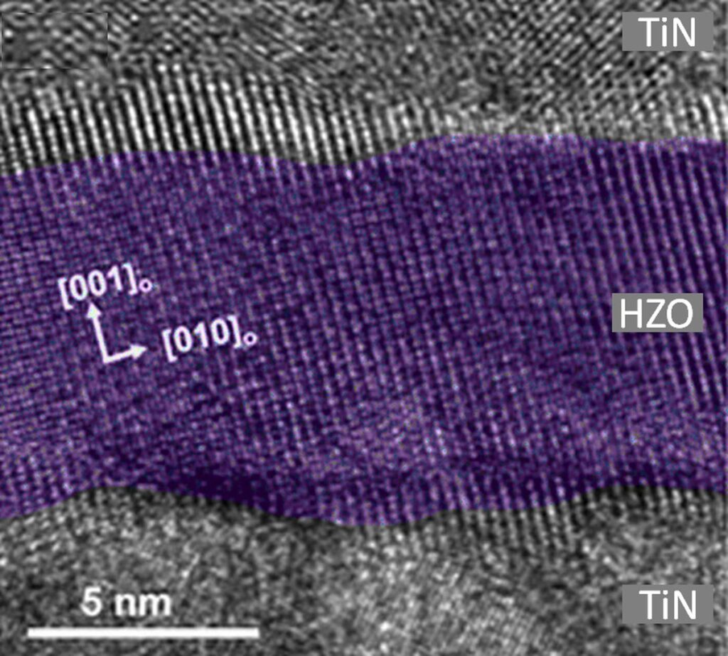
Dielectric materials can be used based on their dielectric ferroelectric, piezoelectric or pyroelectric properties. All four topics were covered in different projects during the last years. The main focus of developing ferroelectric HfO2-based materials is the detailed understanding of the ferroelectric properties in thin doped HfO2 layers. A variety of dopant materials were studied in addition to a mixed Hf1-xZrxO2. Deposition techniques included atomic layer deposition and physical vapor deposition. The ferroelectric orthorhombic Pca21 phase of HfO2 is formed when the material is crystallized with a certain dopant or oxygen concentration at the phase boundary between the monoclinic and the tetragonal/cubic phase and is enhanced through mechanical confinement. Scanning transmission electron microscopy and electron diffraction methods confirmed the structure. Continuous research aims to understand the root cause of this previously unknown phase. Here, dopant and oxygen content, which are directly related to stress and strain in the layer, play an essential role in phase stabilization. A linear relation between strain and the coercive field of the phase transition field was found.
Wurtzite-structured ferroelectric nitrides, such as cation-substituted aluminium nitride, are being developed as a second ferroelectric material for use in devices.
Our competences thereby cover the value chain, from material development to device engineering, structural and electrical characterization, device reliability. The target applications are ferroelectric films for ferroelectric and dynamic random access memory cells (FeRAM and DRAM), high dielectric constant materials for power devices, and diffusion barriers.
Contact

Dr. Uwe Schroeder
Deputy Scientific Director




Dr. Ruben Alcala
Project Manager info@namlab.com

Dr. Roberto Guido
Project Manager info@namlab.com
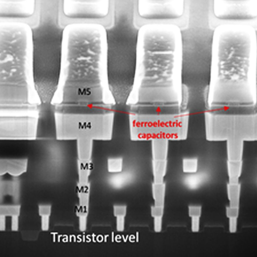
Material and Device Development for Random Access Memory Cells. The main focus of the working group is material and device development ferroelectric and dynamic random access memory cells. We are able to optimize (Hf,Zr)O2 based films for small-scale capacitors in our own clean room. The current focus is on thickness scaling and to understand how parameters like strain dopants and vacacies can impact the properties.
High dielectric constant materials. In modern computer chips, traditional insulating layers like silicon dioxide have become ultra-thin. When SiO₂ gets thinner than roughly one nanometer, electrons leak right through the barrier. By using high-k dielectrics (such as hafnium oxide or zirconium oxide), engineers can use a physically thicker layer that provides the exact same electrical capacitance while stopping current leakage.
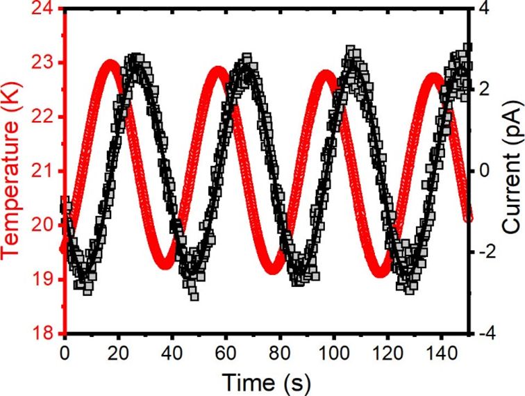
Piezo- and Pyroelectric Materials. The main focus of the work is on a detailed understanding of the pyroelectric properties (PE) in thin doped HfO2 layers. Pyroelectric properties were characterized for various doped HfO2 and Hf1-xZrxO2 films with different thicknesses. A survey of the pyroelectric behavior was undertaken for a wide variety of dopants incorporated into HfO2 including Al, Gd, Sr, and La as well as the Hf0.5Zr0.5O2 composition.

Wurtzite structured ferroelectric nitrides. Wurtzite-structured ferroelectric nitrides, such as cation-substituted aluminum nitride, are among the most promising candidates to develop the next generation of energy-efficient nonvolatile memories. The research at NaMLab focuses on the growth, structural and electrical characterization of cation-substituted aluminum nitride thin films.
Electrical Characterization and Reliability. In order to develop devices for specific applications, a deep understanding of their underlying physics is required. We use a variety of electrical characterization techniques, including access-rate-dependent field cycling endurance and retention measurements, and temperature-dependent characterization from liquid nitrogen to 600°C.

Diffusion Barriers. Various devices require diffusion barriers to improve long-term stability. For this purpose, an atomic layer deposition (ALD) film stack has been developed for use in organic light-emitting diodes (OLEDs), back-end-of-line (BEOL) CMOS and other diffusion-critical applications.
Yearly Events
Namlab Novel High k Application Workshop
D3PO
Dopant and Defect Physics for Device Optimization for Hafnium Oxide based Devices (in cooperation with UAS Munich, CEA LETI, and CEA Saclay, start 2023)
SIDFEM
Strain and Interface Design for the Optimization of Ferroelectricity in the Hf1-xZrxO2 Material System (in cooperation with UAS Munich, start fall 2025)
Ferro4EdgeAI
Zeppelin
Ferroelectric zirconium oxide for piezo- and pyroelectric devices (in cooperation with RWTH Aachen and UAS Munich, finished)
WUMM
Wurtzite Solid Solutions as a New Material Class for Ferroelectric Microelectronics (in cooperation with Univ. Kiel, finished)
Cooperation:
Intel (USA), Sony (Japan), Samsung (Korea), Infineon (Germany/Austria), RWTH Aachen (Germany), Hochschule München (Germany), Science Tokyo (Japan), University of Nebraska (USA), Seoul National University (Korea), North Carolina State University (USA), Penn State University (USA), University Konstanz (Germany), IFW Dresden (Germany), CEA LETI & CEA Saclay (France), University Tokyo (Japan)