NaMLab hosts a dedicated physical characterization toolpark to supplement its core expertise in state-of-the-art material development and electrical characterization. One focus of the physical characterization at NaMLab aims to provide fast-feedback to the technology development in the cleanroom and at research partners.
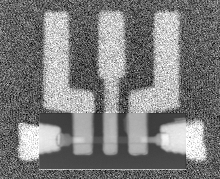
Two high-resolution scanning electron microscopes (HR-SEM) are capable of providing high magnification images down to 10 nm resolution. Our new angle-selective-backscattered electrons detector (AsB) allows to obtain superior material contrast with respect to conventional imaging. Moreover, high channelling contrast can also be achieved, yielding more detailed crystallographic information. A possible application is the localization of nickel silicide junctions placed below metal gates shown in Fig. 1. The high material contrast delivered by the detector allows to precisely image the sharp junctions without saturation of the signal by the electron contribution coming from the overlying metal gates. Furthermore, one SEM is equipped with an energy-dispersive x-ray (EDX) detector to reveal chemical composition of the samples covering almost the entire periodic table. The EDX system is coupled with a newly-acquired Electron Back-Scatter-Diffraction (EBSD) detector, to also yield localized information about crystal structure, phases and textures of nanoscale materials.
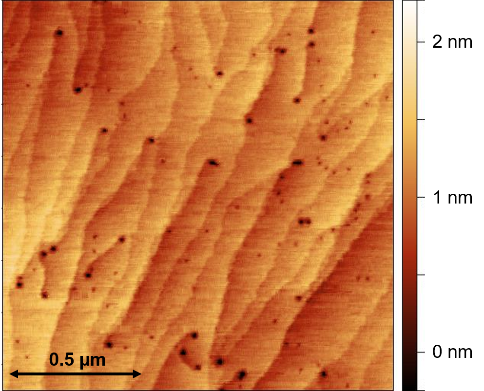
The atomic force microscope (AFM) is routinely used for mapping the surface topography by using contact or tapping mode. Resolution in the order of 2 nm in the scanning direction (X/Y) and below 0.1 nm perpendicular to the scanning direction (Z) can be realized, shown at an example of an epitaxial grown GaN surface in Fig. 2. At NamLab a big variety of special measurement technique is used with a great expertise such as scanning Spreading Resistance Microscopy (SSRM) to map the spatial dopant distribution, conductive AFM (C-AFM) for measuring local leak-age current density, piezo force microscopy (PFM) for analyses of piezo-electric materials by measuring the vertical displacement of the AFM tip in response to an electrical excitation of the sample.
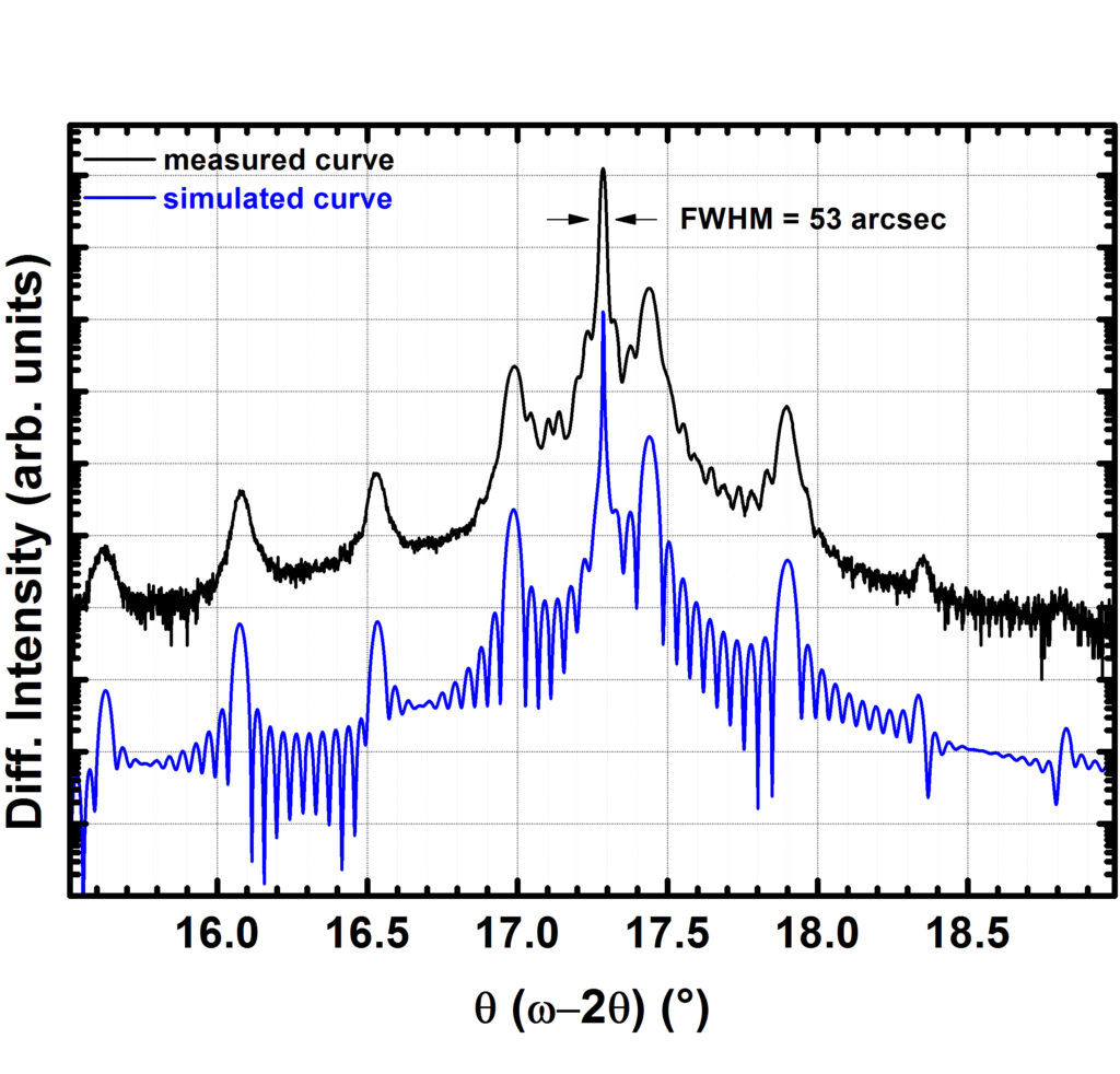
A multifunctional X-ray diffractometer (XRD) is used to yield information about crystal structure. The tool has a resolution of < 40 arcsec and is used for phase analysis, measuring reciprocal space maps, determining the composition of alloys, layer thickness and stress state. A high-resolution X-ray diffraction measurement on a AlGaN/ GaN superlattice structure is shown in Fig. 3.