The purposeful introduction of defects within the Si crystal to tune the properties of electronic devices, for example achieving higher conductivity and a lower parasitic source/drain resistance, has always been a fundamental part of semiconductor technology. This process, called doping, is decisive for the functionality of the material that is defined by acceptor (p-type) or donor impurities (n-type). However, these impurities cause a multitude of problems that counteract on the final device performance such as speed, power consumption and efficiency. At the nanoscale, most of these dopants act as scattering centers in the channel that reduce the mobility of the carriers, and are prone to spatial redistribution due to dopant out-diffusion, and statistical fluctuations.
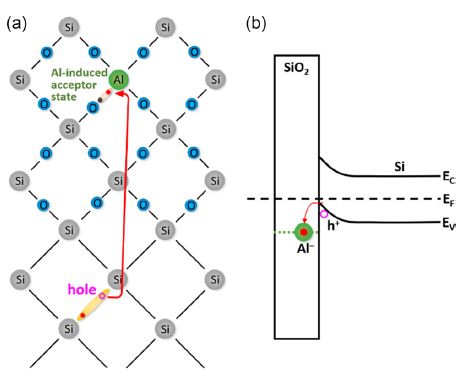
NaMLab is currently working with its research partners to overcome the drawbacks of conventional doping methods at the nanoscale for Si with the concept of Modulation Acceptor doping, with places the defects spatial separated from the channel material. Such a concept was established for silicon nanowires by introducing Al dopants into to the SiO2 dielectric surrounding. The structural properties of the aluminum (Al) atom acting as an acceptor makes it possible for it to be integrated into the SiO2 lattice offering an unoccupied energetic state below the valence band of silicon. The provision of this vacant energy level attracts electrons from silicon that are capable of tunneling to the acceptor states, modifying the behaviour of silicon as p-type with holes as dominant carriers (Fig. 1).
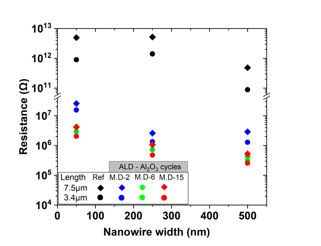
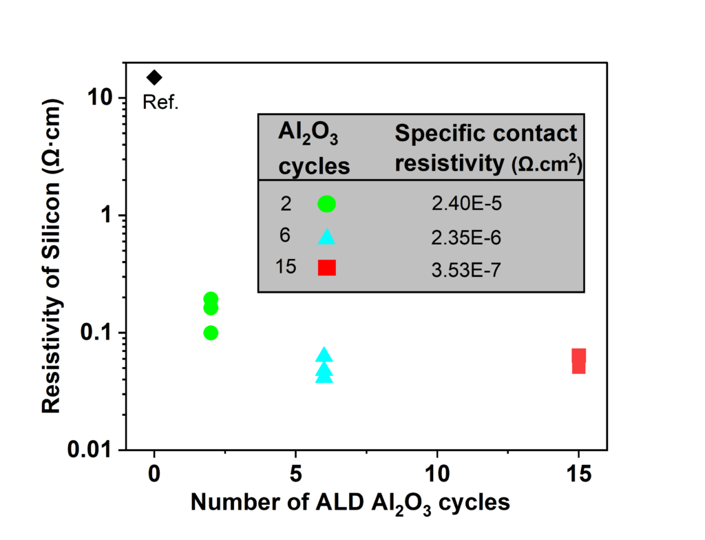
The proof of concept for this approach was demonstrated on Si nanowires fabricated from silicon-on-insulator (SOI) wafers. The modulation doping process involves forming a stack of layers mainly SiO2 and Al2O3 on top of the structured nanowire that functionalizes the Si channel after a thermal activation process. The devices were characterized through electrical measurements by forming metal-silicide contacts. A significant reduction in the electrical resistance of the nanowires was reported (Fig. 2) for varying Al acceptor densities in SiO2. This novel approach has proven to influence both the Si resistivity and the specific contact resistivity that were independently characterized by transfer length measurements (Fig. 3). A carrier density equal to 5E18 cm-³ dopant atoms has been achieved experimentally. As for classical doping methods, a broad range can be defined by varying the number of atomic layer deposited (ALD) Al2O3 cycles. Also, it has been shown that the charged defects in the shell have an additional effect on the Schottky contact properties of the silicon nanowires. At present, the concept is being further developed for application in Junctionless nanowire transistors.

Cooperation:
Technische Universität Bergakademie Freiberg (Germany), Australian National University (Australia).