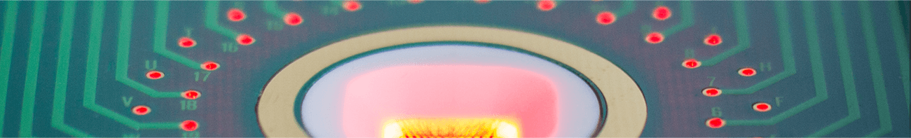
The central aim of the research on Resistive Switching Devices is the development of materials and device structures, capable of changing their electrical resistance or capacitance by applying external voltages. The resistive memory device – the so called ReRAM – is one of the potential candidates for the realization of novel memories, since it is characterized by very fast access times, non-volatility, and low power consumption. A further interest for the adoption of these devices – also referred to as memristors – is the application of such reconfigurable devices in neuromorphic nano-circuits, exhibiting the unified functionality of logic and memory in one device. NaMLab’s activities cover the deposition and modification of dielectric thin films and electrode layers, the physical and electrical characterization as well as the modeling of the switching properties.
NaMLab’s research focuses on niobium oxide (NbOx)-based resistive switching devices. By variation of the fabrication process, electrode materials and thin film composition a large variety of different switching characteristics could be obtained.

Fig. 1 depicts the measured impedance over frequency of a NbOx / Al2O3 -based bi-layer device. For low frequencies the analogue resistive switching behavior results in a splitting into different impedance states that are determined by the different conductance states representing the stored data. At high frequencies above 105 Hz the impedance is mainly determined by the capacitive part which naturally results from the metal-insulator-metal structures. Finally, there is a transition region in which we can observe memcapacitive properties – that is a change of its capacitance depending on the internally stored memory state. The combination of resistive and capacitive switching effects in these devices gives rise to a rich dynamic behavior that we utilize in the conception of novel devices such as neuro-transistors or synapses for unconventional and neuromorphic computing. For example, the data shown in Fig. 2 depicts the potentiation and depression behavior of an artificial synapse for both the memristive and memcapacitive part. Physics-based models that are able to describe the electrical device behavior which are further used in circuit simulation. Finally, we integrate the devices together with transistors as provided by project partner TUD, or manufacture stand-alone cross-bar arrays as shown in Fig. 3.

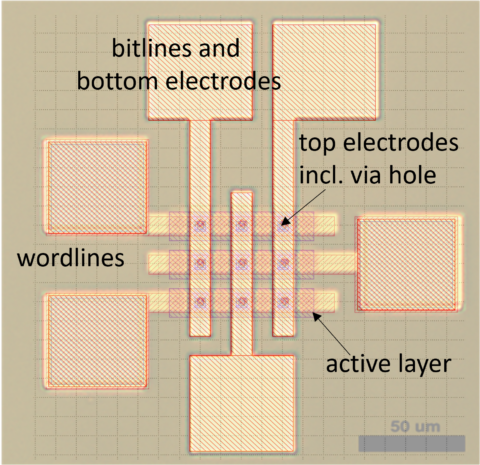
Fig. 3: Top-down SEM image of a 64kbit ReRAM test chip. The orange regions show the metal 5 layer of the underlying 28nm CMOS chip, while the green stripes are the top-electrodes manufactured at NaMLab.

Cooperation:
TU Dresden (Germany), Leibniz Institute for High Performance Microelectronics (Germany).