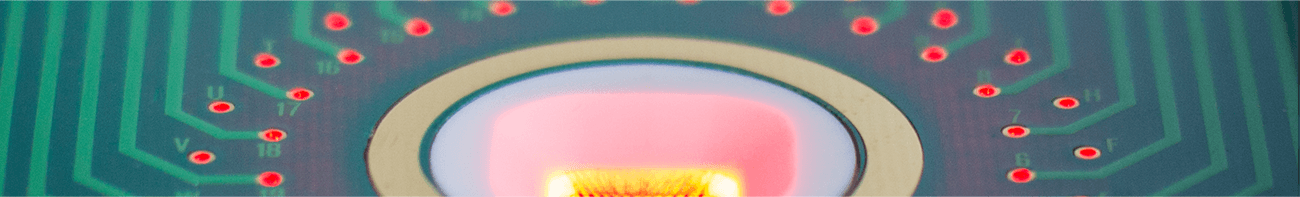
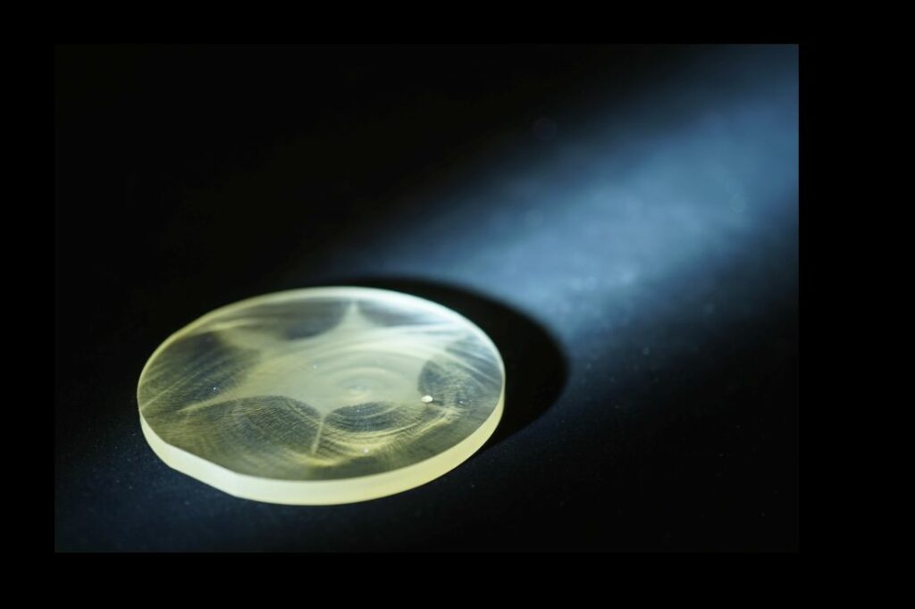
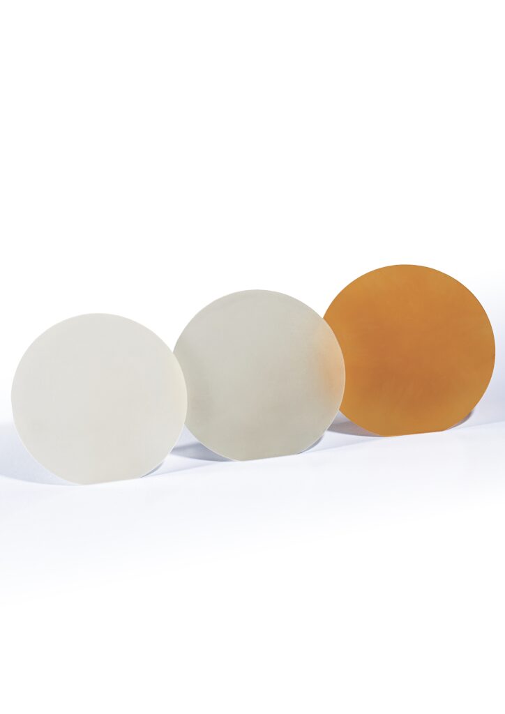
Since 2011, NaMLab is belonging to a small but elite group of bulk-GaN growers. It cooperates on-site with Freiberger Compound Materials (FCM) in Freiberg and owns a modified and optimized state-of-the-art vertical HVPE reactor. The focus of the research and development is on the growth of several millimeters thick GaN-crystals (Fig. 1). So far, crack-free 3″ crystals can be grown reliably and cut into distinct 2” wafers (Fig. 2). Different dopants are applied to adjust the electrical properties between n-type and semi-insulating. Besides upscaling to higher diameters, the optimization of the lattice properties, e.g. the lattice bow, is of major interest.
Due to the hetero-epitaxial approach of the HVPE process, bowing of the crystallographic lattice planes towards the crystal edge can generally not be avoided. Recent developments of the growth process promise the lattice properties (e.g. lattice radius of curvature) to be competitive to homo-epitaxial approaches.
N-type conductivity above the unintentional doping level (charge carrier concentrations not larger than 5 x 1016 cm-3) is achieved by using Silicon (Si) as a dopant.
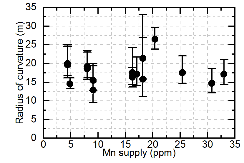
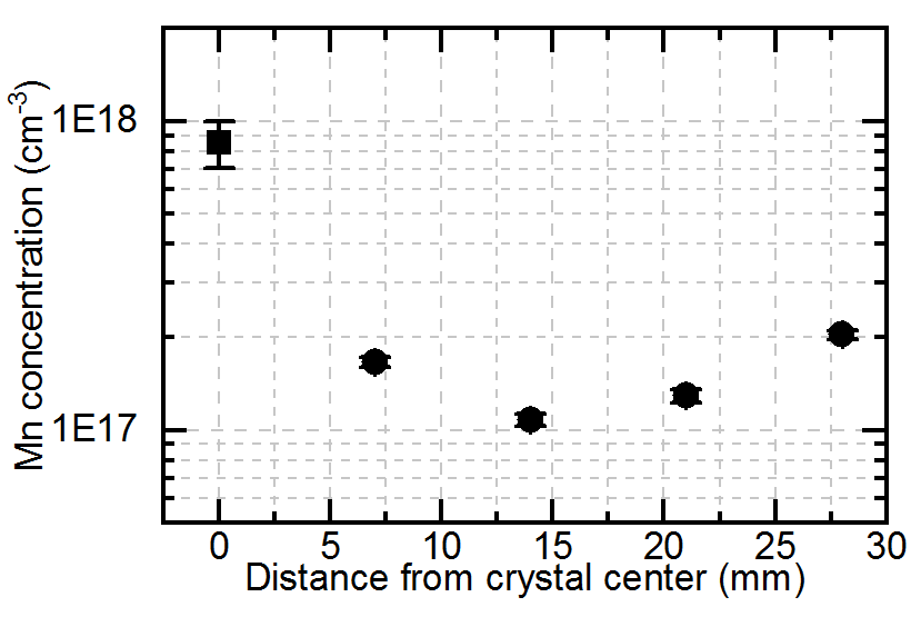
On the contrary, semi-insulating GaN crystals have been established by doping with deep acceptors, especially Manganese (Mn) by a solid-state method. High doping concentrations above 1018 cm-3 are already possible without deterioration of the lattice properties (Fig. 3). Additionally, a bubbler setup using a metal-organic (MCp)2Mn precursor has been established to improve the flexibility and control of the Mn doping. While the dopant distribution perpendicular to the crystal surface is uniform, there is a large lateral concentration variation for both Mn doping approaches (Fig. 4).
Future targets are the improvement of the lateral doping homogeneity as well as increasing the doping concentration for the bubbler doping while maintaining the high lattice quality. Furthermore, the suitability of other metal-organic dopants like Cp2Fe (ferrocene) or DEZn (Diethylzinc) will be evaluated for the fabrication of semi-insulating GaN.
In general, the efforts towards a further improvement of the crystal lattice bow, better understanding of dopants incorporation and increase of the crystal diameter will be continued.
In 2022 a planetary MOVPE reactor owned by NaMLab was installed expanding further the on-site cooperation with FCM. The MOVPE reactor was successfully started up. The development of MOVPE-GaN templates designated to be used as starting seeds in the HVPE GaN crystal growth has started.

Cooperation:
Freiberger Compound Materials GmbH, Freiberg (Germany)