HfO2-based ferroelectric memories are long-term contenders for ultra-fast, low-power and non-volatile memory technologies. The electric polarization reversal in ferroelectric thin films is adopted in different memory devices. While the write operation is always conducted by applying an electric field in either polarity to the ferroelectric film, the read operation distinguishes three main concepts. In the FeRAM mode, the displacement current of a ferroelectric capacitor (FeCAP) is directly measured during polarization reversal, leading to a destructive read operation. In contrast, in the ferroelectric tunneling junction (FTJ) the polarization state dependent leakage current is measured and is indicative for the stored data. Finally, in ferroelectric field-effect transistors (FeFET) the information is stored as a polarization state of the gate dielectric and can be read non-destructively as a shift of the threshold voltage of the transistor.
In collaboration with GlobalFoundries and Fraunhofer IPMS FeFET devices were successfully implemented in a 28 nm gate-first super low power (28SLP) CMOS technology platform using only two additional structural masks. In our work we concentrate on the electrical characterization and modeling of the FeFET. The distinct electrical characteristics of these novel devices are analyzed in detail. Target is the comprehensive understanding of the interplay between different physical mechanisms that influence important memory characteristics such as cycling endurance or data retention as well as switching voltage and times. Fig. 1 reports the measured trade-off between the switching voltage and switching time for the program and erase operation of fully CMOS integrated FeFET devices. From this data it is possible to determine the optimum operation conditions and/or the retention time by extrapolation to 0 V gate voltage.
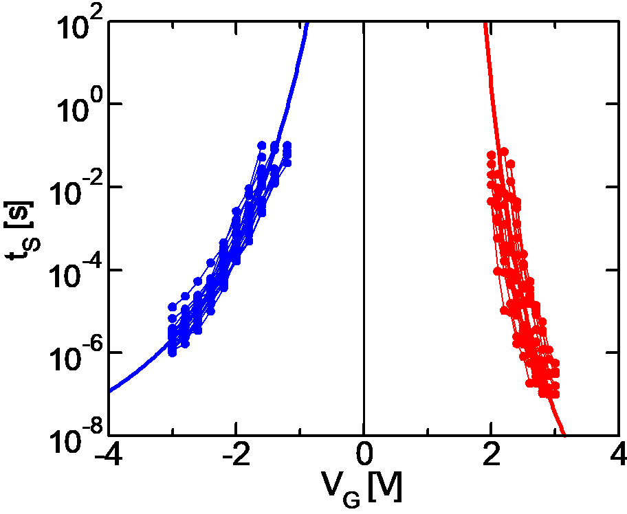
Fig. 2 depicts the superior memory window of up to 1.7 V that was measured in a passive array of 63 FeFET devices featuring a 9 nm thick ferroelectric film. The thickness of the ferroelectric has an impact on the memory window but also on the internal electric fields that are decisive for the data retention. With our results we aim at further optimizing the FeFET technology and to support our start-up company FMC (Ferroelectric Memory Company, www.ferroelectric-memory.com) targeting at the commercialization of the FeFET-based memory, which was developed in Saxony during the recent years. Besides device characterization and modeling we further engage in the development of memory cells and operation schemes that match the specific needs of the ferroelectric devices. Fig. 3 shows the schematic circuit diagram of our recently proposed 2 transistor 1 capacitor ferroelectric memory cell for the adoption of small scaled FeCAPs or FTJs.
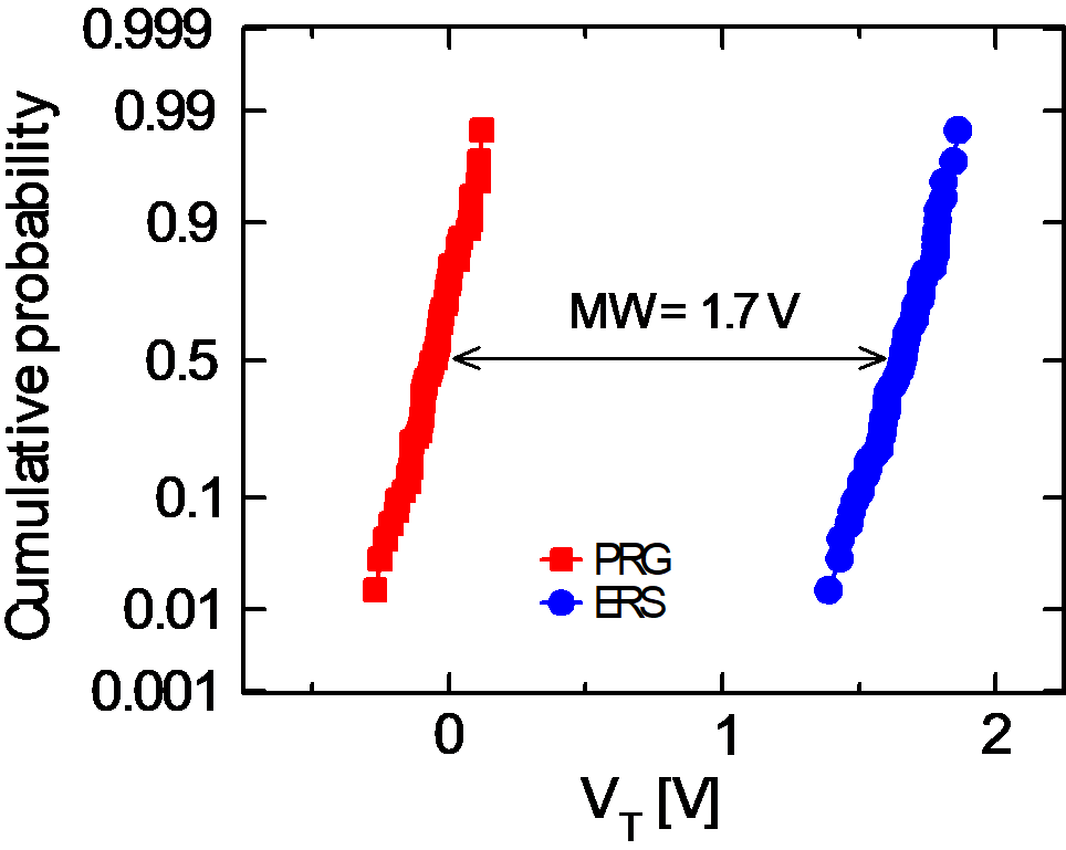
Fig. 2: Cumulative probability plot of low-VT and high-VT state of 63 FeFET devices measured in a passive memory array. The 9 nm thick ferroelectric layer exhibits a mean memory window of 1.7 V. 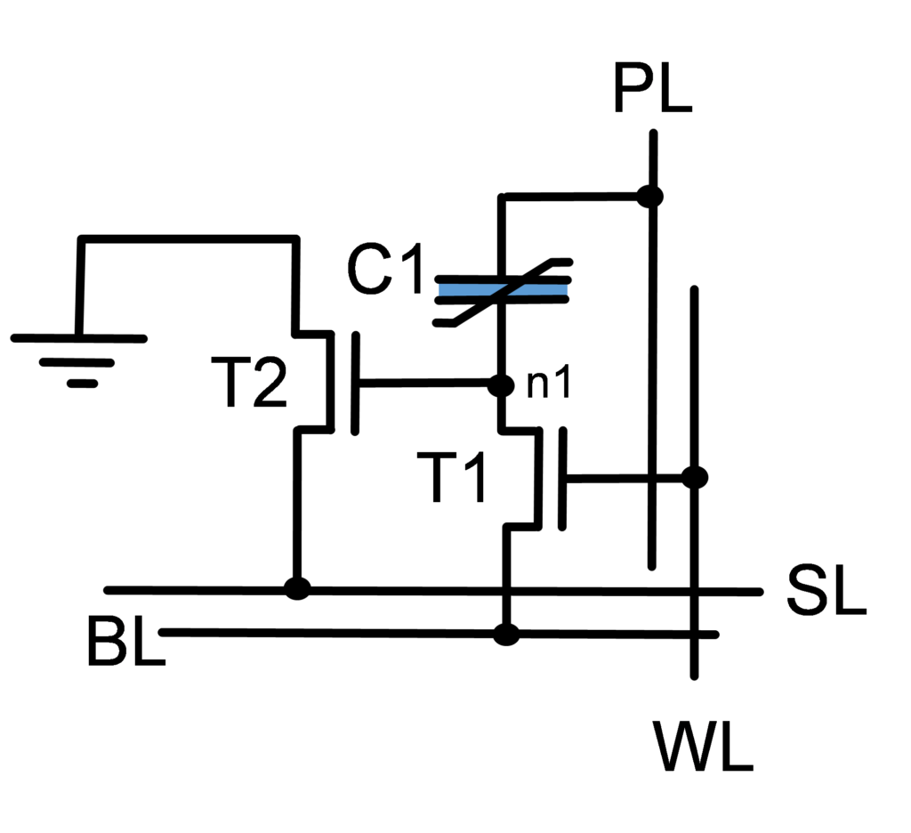
Fig. 3 A 2T1C ferroelectric memory cell for small scaled planar ferroelectric capacitors and ferroelectric tunneling junctions (FTJ). In this concept T1 is the access transistor while T2 provides a cell-internal signal gain.

Cooperation:
GLOBALFOUNDRIES (Germany/USA), Fraunhofer IPMS-CNT (Germany), FMC (Germany)