
With classical scaling of CMOS transistors according to Dennard ́s scaling rules running out of steam, new possibilities to increase the functionality of an integrated circuit at a given footprint are becoming more and more desirable. A promising concept in this sense is to increase the functionality of a system by keeping the number of individual elements the same.
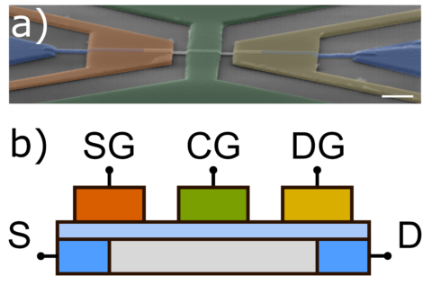
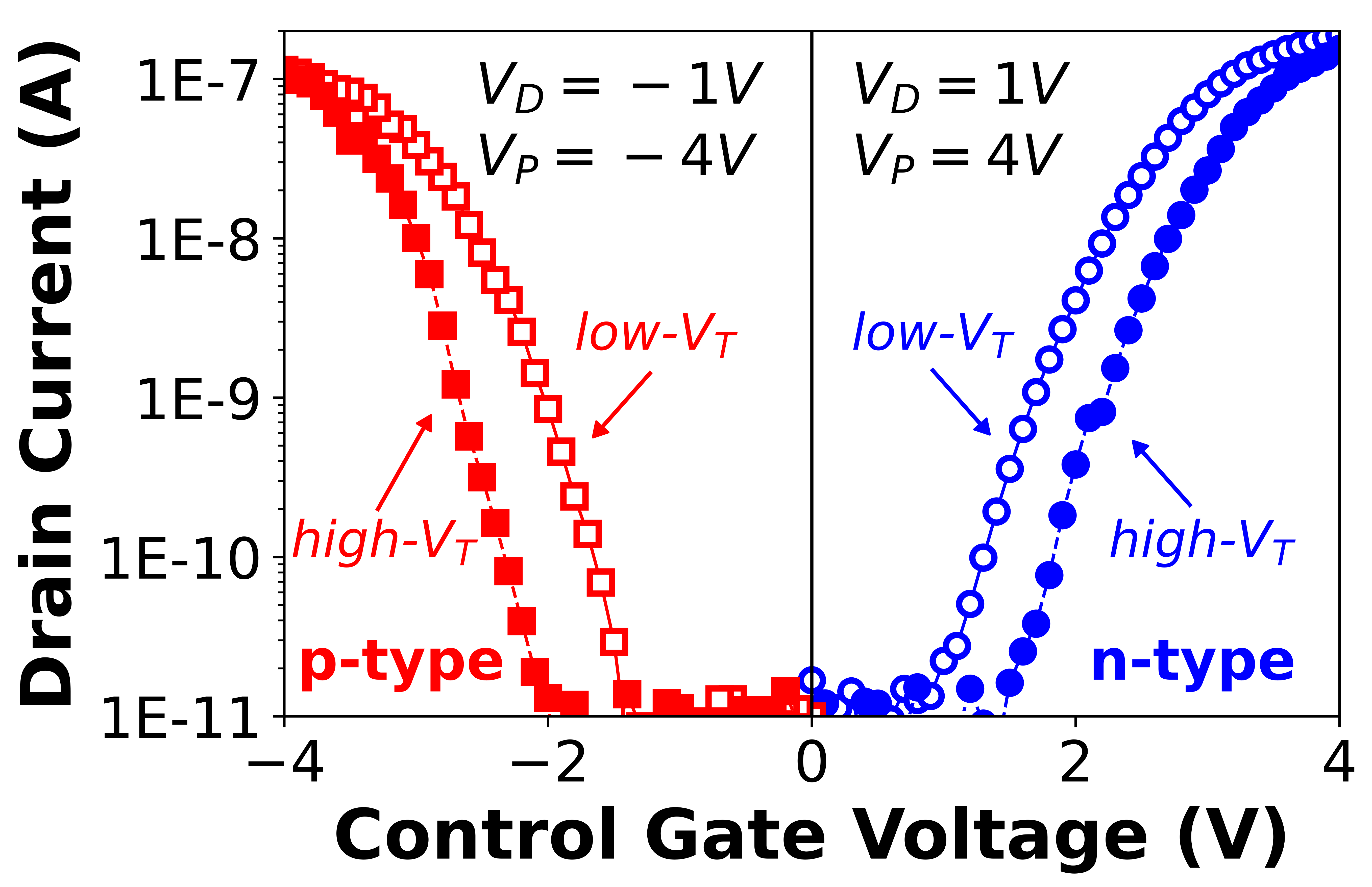
The reconfigurable field-effect transistor (RFET) can provide such a feature, as it is an electronic device whose conduction mechanism can be reversibly reconfigured between n-type and p-type operation modes. In its most versatile variant, three-independent gates are patterned over a nanoscale channel, whereby the two outer gate electrodes directly control carrier injection across the Schottky junctions at source and drain (Fig. 1). The device can be operated either at the source-sided gate or at the central gate, which corresponds to a high-VT, or low-VT mode, respectively (Fig. 2). As both gates are placed in series, the transistor embodies the wired-AND function. Importantly, RFETs do not rely on chemical doping caused by impurities, but rather on electrostatic doping, i.e. the generation of mobile carriers via an external potential.
Over the last years, NaMLab has focused on the transfer of this lab technology originally demonstrated on silicon nanowires to more mature industrial processes and materials. Thereto, a robust top-down route for fabrication on SOI substrates using electron beam lithography and reactive ion etching was setup. The gate sizes of the individual devices were adjusted to cover for some variability in the silicide formation. As a result, lab devices can be fabricated with sufficient yield and throughput to perform statistical analysis, first reliability investigations, and the demonstration of functional logic gates. Also, the operation of the devices at high and low temperatures has been investigated.
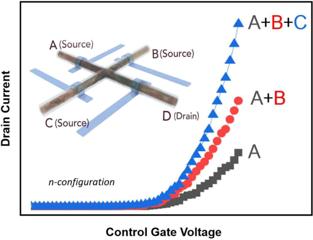
Moreover, the cross-shape RFET was demonstrated as a radically new device variant based on the of unique transport features of Reconfigurable Transistors. This device utilizes multiple source and drain contacts on a common-body, each being individually gated, thereby facilitating transistor-level current routing through each of its branches, embodying a wired-OR functionality (Fig. 3). Providing linear addition of the current of all sources at the single drain, the device concept has potential for flexible signal routing or neuromorphic circuit applications.

Cooperation:
RWTH Aachen (Germany), CNRS-LAAS Toulouse (France), INL ECL Lyon (France), TU Wien (Austria), AMO GmbH (Germany)