
The III-V compound semiconductor Galliumnitride (GaN) has outstanding intrinsic material properties for power device applications. NaMLab’s GaN device development is focused on electronic power devices with high voltage operation. The High-Electron-Mobility-Transistor (HEMT) concept features a 2 dimensional electron gas (2DEG) at the AlxGa1-xN/GaN heterojunction interface. It represents the backbone of GaN power transistors with planar or lateral current conduction close to the wafer surface. The material for industrial device fabrication consists primarily of MOCVD grown GaN on Si(111) substrates with diameter of 200 mm.
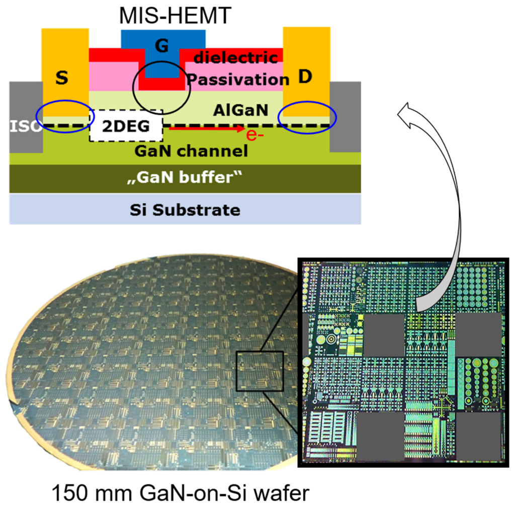
A HEMT technology based on contact lithography for 150 mm wafers is utilized for material characterization and device development in cooperation with external partners (Fig.1). NaMLab is working on process modules for improving overall device performance, stability and reliability. We investigate the integration of a high-k dielectric material underneath the gate electrode to fabricate a Metal-Insulator-Semiconductor (MIS)-HEMT. Process engineering on the (Al)GaN surface prior to the deposition of the dielectric as well as post-annealing of the gate structures improves importantly the threshold voltage stability. An alternative ohmic contact module based on Ta/Al metal bilayers was investigated and compared to the mainstream Ti/Al/Ni/Au contacts. Material engineering resulted in low-resistance Ta/Al/TiN-ohmic contacts (Rc < 1 Ω.mm) at much lower annealing temperatures (≤ 600°C), which are gold-free and enable a higher integration flexibility. Currently, we explore the integration of ferroelectric materials in the gate architecture of HEMT devices aiming to tune the threshold voltage in dependence of the spatial orientation of polarization, comparable to Silicon-based ferroelectric field-effect transistors.
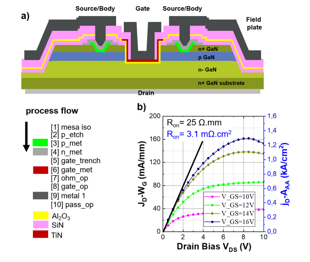
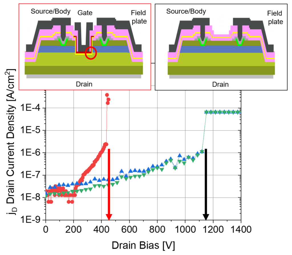
Another device concept is related to vertical GaN power devices, having the advantage of an almost area-independent scaling of the breakdown voltage. NaMLab has developed a vertical GaN MOSFET device with trench gate configuration and device channel along the vertical sidewall of the trench (Fig 2.). The process integration has been adapted to full vertical devices on 2-inch free-standing GaN substrates with backside contact. Power demo-devices with multiple gate trenches connected in parallel showed threshold voltage > 3V and low specific on-resistance of 3 mΩ.cm2. Utilizing a low doped drift layer with thickness of 10 µm and a conformal gate dielectric of 45 nm Al2O3, the MOSFET exhibits a pre-mature breakdown at 450 V most likely in the trench corners (Fig. 3). Contrarily, the lateral device termination with field plate structure on the device mesa isolation shows non-destructive breakdown at 1.1 kV.

Cooperation:
Freiberger Compound Materials GmbH, Freiberg (Germany), TU Dresden (IHM) (Germany), TU-BA Freiberg (Germany), X-FAB (Germany)