Electrical measurements are essential for the characterization of the materials that are used to create electronic devices and circuits. NaMLab adopts a broad spectrum of electrical measurement techniques and analysis methods for device characterization. This includes capacitance measurements, such as C(V), C(T) and C(f), current measurements with down to femto-ampere resolution at temperatures between 5 K and 450 K and voltages up to 3000 V. Samples can be analyzed by direct probing on wafer level using single probes, probe cards or special RF-probes. Package level testing can be performed for long-term reliability characterization or for the adoption of our devices in test-circuits. In addition, carrier lifetime measurements are available on substrates with Microwave Detected Photoconductivity.
The established methods at NaMLab include:
• Analysis of single devices (logic and power transistors), circuits or
memory cells by static and pulsed measurements
• Determination device characteristics by C-V and I-V measurements
• Determination of doping profiles by scanning spreading resistance
Microscopy (SSRM)
• Reliability characterization of dielectrics, devices and circuits
• Defect characterization by charge pumping and charge trapping
analysis and defect spectroscopy
• Measurement of charge carrier mobility with Hall and split-C(V)
• Pulsed and high frequency measurements
• Development of novel characterization methods and test structures
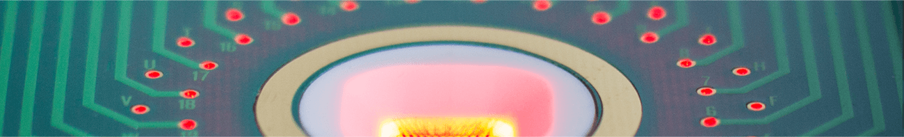
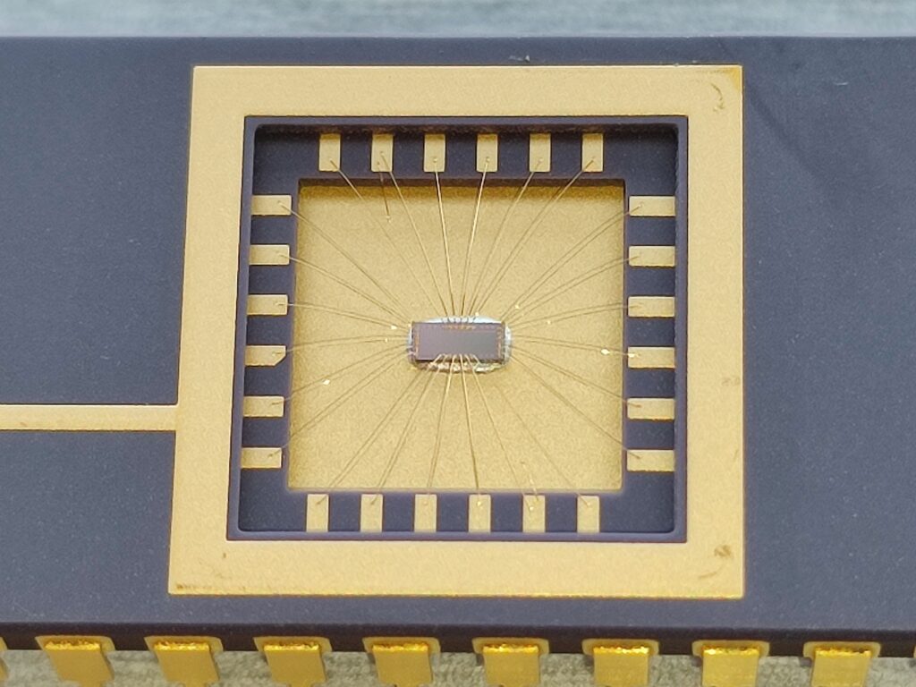
Characterization of memory arrays closer to system level are performed to develop new application scenarios. Fig. 1 shows a packaged 64kBit FeFET memory test chip. It was designed for the investigation of radiation hardness of this technology at UZL in Leuven, Belgium.
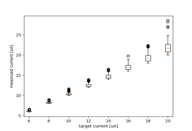
In another work, special operation modes such as target programming for analogue and multi-level state storage in conventional FLASH memory arrays were investigated, targeting at the realization of analogue vector matrix multiplication in FLASH-arrays. Fig. 2 shows the measured distribution of on-currents of 720 SONOS cells programmed to eight different levels.
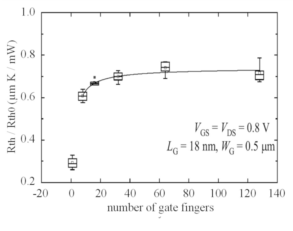
Finally, based on a novel RF-characterization methodology the impact of self-heating effects on the reliability of 22nm FD-SOI transistors was investigated. Fig. 3 shots the extracted thermal resistance of a MOSFET device structure depending on its layout – in this case the number of gate fingers.