


The growth of GaN/AlGaN heterostructures by molecular beam epitaxy (MBE) focuses on the exploration of fundamental material properties and device concepts. The MBE material represents an ultra-pure reference with an irreducible unintentional oxygen level of 2×1016 cm-3, which is achieved by employing optimal growth conditions. In such ultra-pure GaN/AlGaN stacks, the surface potential is pinned deep inside the bandgap, which leads to the absence of a two-dimensional electron gas (2DEG) at room temperature and in dark environment. However, such a 2DEG can be generated under illumination with ultra-violet (UV) light. This discovery represents a novel generation of normally-off and UV-sensitive lateral devices.
MBE growth of ultra-pure GaN-based heterostructures on bulk GaN substrates has contributed to the demonstration of record-breaking narrow excitonic line widths and the optical detection of Landau level splitting. The feasibility of MBE-grown heterostructures grown on bulk GaN for high-power radio frequency applications is part of our current research and cooperation with R&D partners.




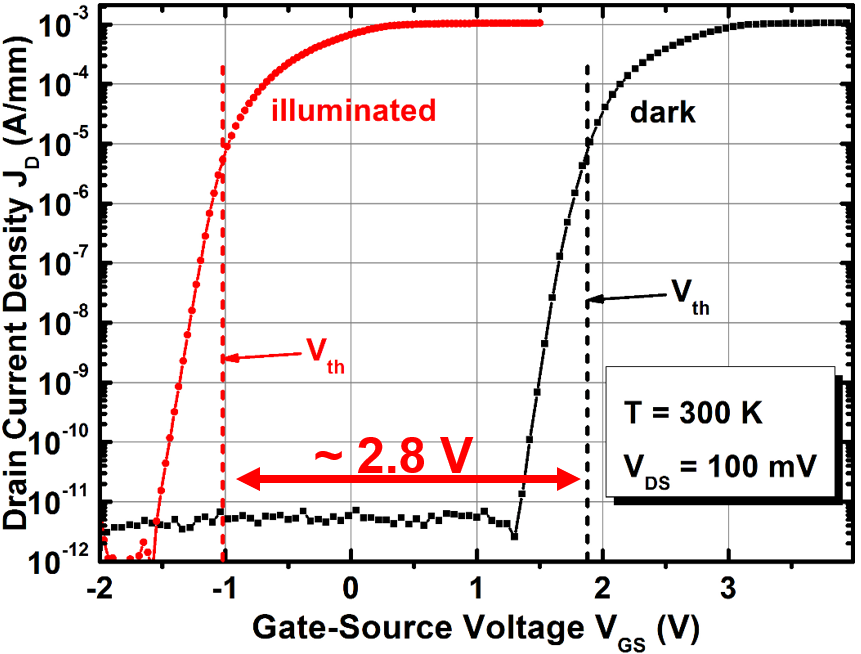
Normally Off GaN HEMT Stacks Transfer characteristics of a lateral field-effect transistor (FET) fabricated from an ultra-pure GaN/AlGaN stack grown by MBE. In dark environment, no 2DEG is present and the FET is normally-off, while under illumination it works in depletion mode.

MBE growth of ultra-pure GaN/AlGaN hetrostructures. fabrication of lateral test structures text missing
Low-temperature characterization of electrical and optical properties, characterization of structural surface and bulk properties text missing