


Since 2011, NaMLab is belonging to a small but elite group of bulk-GaN growers. It cooperates on-site with Freiberger Compound Materials (FCM) in Freiberg and owns a modified and optimized state-of-the-art vertical hydride vapor phase epitaxy (HVPE) reactor. The focus of the research and development is on the growth of several millimeters thick GaN-crystals. Due to the hetero-epitaxial approach of the HVPE process, bowing of the crystallographic lattice planes with respect to the crystal surface can generally not be avoided. Through major advances in understanding lattice bow and strain reduction, the lattice radius of curvature increased, while the spread of the radius of curvature decreased, for the grown crystals. Today it is possible to run series with a yield above 90% for GaN crystals with a diameter of 3 inches that are cut into distinct 2” wafers.
Different dopants are applied to adjust the electrical properties between n-type and semi-insulating. N-type conductivity above the unintentional doping level (charge carrier concentrations not larger than 5 x 1016 cm-3) can be reliably adjusted up to 5 x 1018 cm-3 by using Silicon (Si) as a dopant. Doping with deep acceptors (Mn, Fe and Zn) was investigated to achieve semi-insulating GaN crystals. A solid-in-liquid doping method was shown to be favorable to achieve Mn and Zn concentrations above 1 x 1018 cm-3 without deterioration of the lattice properties. Fe doping was successfully achieved by a solid-state doping method.
The on-site cooperation with FCM was further expanded in 2022 when a planetary MOVPE reactor owned by NaMLab was installed. 3” and 100 mm MOVPE-GaN templates used as starting seeds in the HVPE GaN crystal growth have been established.
Contact

Dr. Alexander Ruf
Senior Scientist
E-Mail: alexander.ruf[at]namlab.com

Dr. Friederike Zimmermann
E-Mail: friederike.zimmermann[at]namlab.com

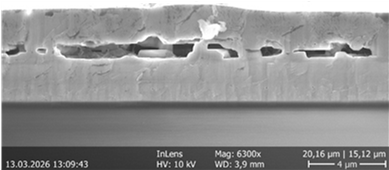
Epitaxial Growth of GaN layers by MOVPE. A novel approach of in-situ formation of a buried porous layer for strain management is currently under development (Fig. 4). Future tasks are the increase of the template diameter and strategies for defect and strain management, in functional interplay with HVPE crystal growth.
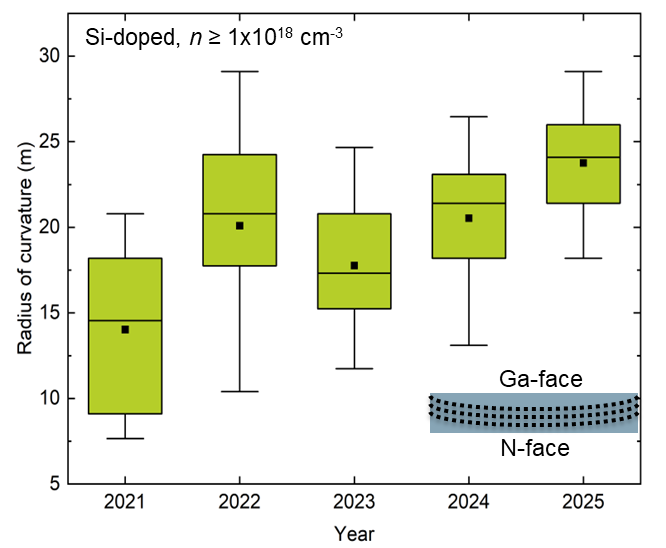
Figure: Over the last five years the mean lattice radius of curvature for Si-doped 3” GaN crystals was increased, simultaneously the spread of values was decreased. The lattice radius of curvature is now consistently above 20 m resulting in yields >90% for crack free crystals.
Epitaxial growth of GaN crystals by HVPE Focus on doping of GaN crystals and characterization of GaN by optical and electrical characterization. The efforts towards lower dislocation densities, further improvements of the lattice bow, a better understanding of the dopant incorporation and an increase of the crystal diameter will be continued.
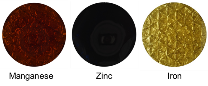
Figure: Central area of 3” GaN crystals doped by a solid-in-liquid approach for manganese and zinc and a solid state approach for iron.
Reduction of Strain GaN crystal. Over the last five years the mean lattice radius of curvature for Si-doped 3” GaN crystals was increased, simultaneously the spread of values was decreased. The lattice radius of curvature is now consistently above 20 m resulting in yields >90% for crack free crystals.
Figure: SEM cross section of a MOVPE GaN layer showing successful formation of a porous interlayer.