


With classical CMOS transistor scaling according to Dennard’s law running out of steam, new ways to increase the functionality of an integrated circuit within a given footprint are becoming increasingly desirable. A promising concept in this regard is the monolithic co-integration of emerging technologies with CMOS to increase a system’s functionality without scaling of the individual feature sizes. The focus of our work is thereby on novel transistor technologies utilizing CMOS-compatible material systems.
A main focus of the group is the polarity-controllable reconfigurable field-effect transistor (RFET), which is a Schottky barrier-based electronic device whose conduction mechanism can be reversibly switched between n-type and p-type operation modes. Unlike classical MOSFETs, the benefit of these devices is evident only at the circuit level, e.g., by combining multiple functions into a single polymorphic logic gate. Beyond RFETs, junctionless transistors, ferroelectric transistors, and resonant tunneling devices are also currently under investigation.
Our competences thereby cover the entire value chain, from material and device engineering, electrical characterization, reliability, TCAD and Verilog-A modelling, to the design and layout of functionality-enhanced circuits. Target application domains include low-power edge computing and artificial intelligence, smart analog sensors, and hardware security, as well as cryo- and quantum electronics.
Contact

Dr. Jens Trommer
Senior Scientist
E-Mail: info[at]namlab.com






Dr. Giulio Galderisi
Project Manager info[at]namlab.com
Material and Device Development for Reconfigurable Field Effect Transistors. The main focus of the working group is device, material, and circuit development of emerging reconfigurable field effect transistors. We are able to fabricate small-scale device and circuit demonstrators in our own clean room. The current focus is on new transistor geometries, low-bandgap and BEOL-compatible channel materials, as well as on integrating non-volatile memory elements directly into the RFET.
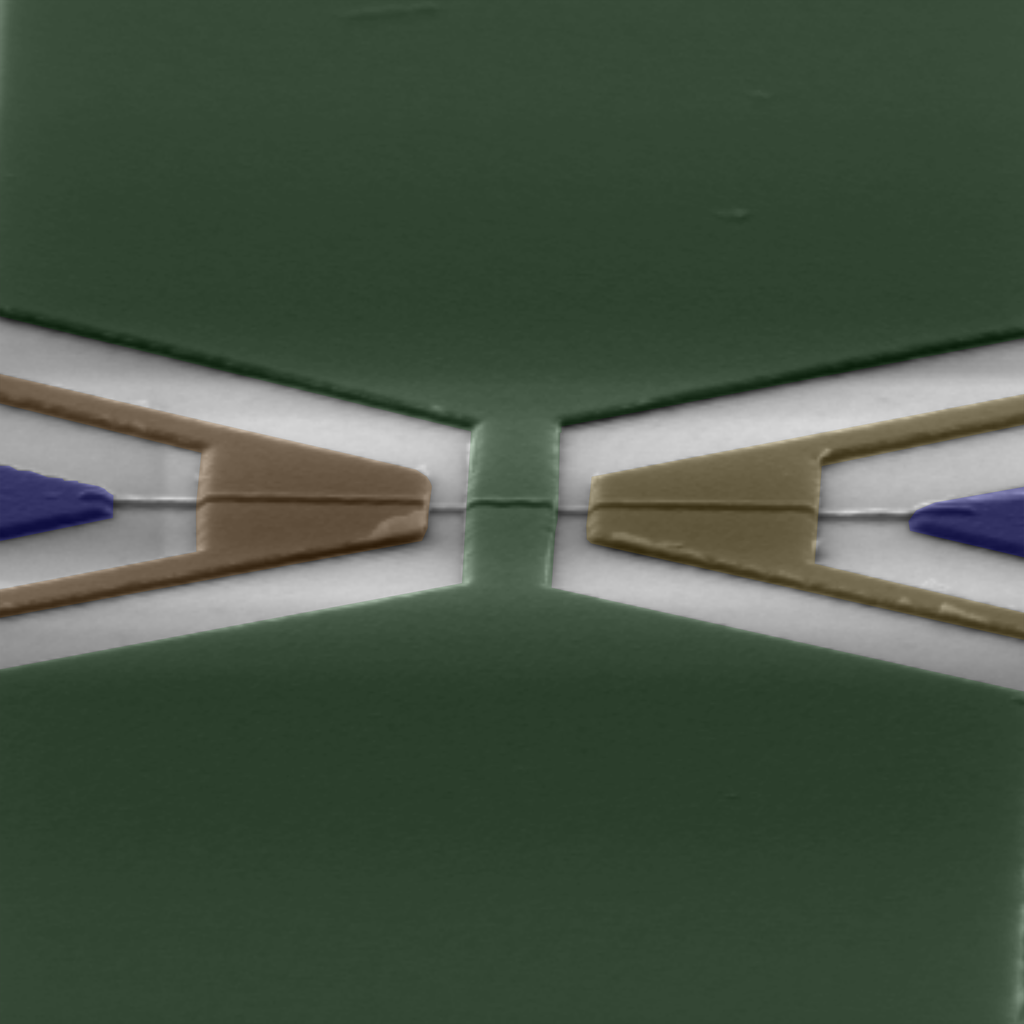
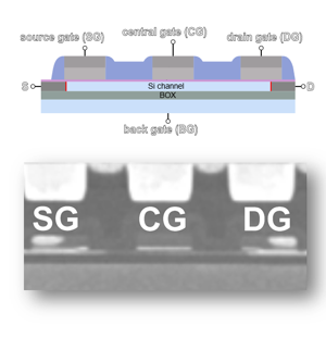
Design Enablement and Circuit Design for Reconfigurable Transistors on a 22nm FDSOI Platform. In a collaborative effort with GlobalFoundries Fab 1 in Dresden, we demonstrated that RFETs can be seamlessly transferred to an industrial FDSOI technology. We support this transfer by design enablement activities, such as transistor modeling, cell design, and library characterization. Further, we conceptualize digital and analog circuit design for a variety of applications, including hardware security, artificial intelligence, and smart analog sensors.
Modulation Acceptor Doping for Cryogenic Applications. Together with our international partners, we have found that electrostatic doping can not only be applied via an external signal, as in RFETs, but also achieved through careful defect engineering of the semiconductor channel’s surrounding dielectric. This way, doping-free transistors can be created in silicon technology, enabling high mobilities at cryogenic temperatures and being perfectly suited for applications in quantum technologies.


Resonant Tunneling Devices for Low-Power Applications. Resonant band-to-band tunneling is a potential approach to lowering the power consumption of transistors by pushing the subthreshold swing below the thermal limit of 60 mV/dec at room temperature. In the QUANTZ project, we fabricate such devices based on layered double SOI substrates.
Electrical Characterization and Front-End-Line Reliability. To push emerging devices to the application level, a deep understanding of their underlying transport physics is required. We conduct a variety of electrical characterization techniques, including DC and RF characterization, temperature-dependent characterization down to 1.8 K, and front-end reliability tests (HCI, BTI, TDDB).
Running Projects: EU SENSOTERIC, BMFTR DI-Re-Design, SecuReFET, QUANTZ, Active-3D.
Closed Projects: EU FVLLMONTI, BMBF CirroStrato, PARFAIT-II, MADSinano, ReproNano I-III
Cooperation:
RWTH Aachen (Germany), CNRS-LAAS Toulouse (France), INL ECL Lyon (France), TU Wien (Austria), AMO GmbH (Germany)